


Analog Devices Inc. AD5691R、AD5692R、AD5693R nanoDAC+ DAC
ADI AD5691R、AD5692R、AD5693R nanoDAC+®デジタル・アナログ・コンバータ(DAC)は、低消費電力、シングル・チャンネル16/14/12ビットのバッファ電圧回路DACです。2.5V内蔵リファレンスがデフォルトでオンになっており、2ppm/°Cドリフトを提供します。出力スパンは0V~VREF または0V~2 ×VREFに設定することができます。全てのデバイスは、2.7V~5.5Vの単電源で動作し、設計によって単調増加性が保証されています。本デバイスは、2.00mm × 2.00mm、8ピンLFCSPまたは10ピンMSOP を採用しています。内部パワーオン・リセット回路により、電源投入時にDACレジスタにゼロ・スケールを書き込み、その間、内部出力バッファはノーマルモードで構成されます。AD5693R/AD5692R/AD5691Rは、デバイスの消費電流を5V時2μA(最大)に低減するパワーダウンモードを備え、出力負荷をソフトウェアで選択する機能を提供します。AD5693R/AD5692R/AD5691RはI2Cインターフェースを使用しています。また、いくつかのオプションでは、非同期のRESETピンとVLOGIC ピンも備えており、1.8V互換が可能です。
The devices are available in a 2.00mm × 2.00mm, 8-lead LFCSP or a 10-lead MSOP. The internal power-on reset circuit ensures that the DAC register is written to zero scale at power-up while the internal output buffer is configured in normal mode. The AD5693R/AD5692R/AD5691R contain a power-down mode that reduces the current consumption of the device to 2μA (maximum) at 5V and provides software selectable output loads. The AD5693R/AD5692R/AD5691R use an I2C interface. Some device options also include an asynchronous RESET pin and a VLOGIC pin, allowing 1.8 V compatibility.
特徴
- 2mm × 2mm, 8-lead LFCSP Ultra-small package
- ±2LSB maximum at 16 bits High relative accuracy (INL)
- 2ppm/°C typical Low drift, 2.5V reference
- 2.5V or 5V Selectable span output
- ±0.06% of FSR maximum Total unadjusted error (TUE)
- ±1.5mV Maximum offset error
- ±0.05% of FSR maximum Gain error
- 0.1nV-sec Low glitch
- 20mA High drive capability
- 1.2mW at 3.3V Low power
- 1.8V to 5.5V Independent logic supply
- −40°C to +105°C Wide operating temperature range
- Robust 4kV HBM ESD protection
アプリケーション
- Process controls
- Data acquisition systems
- Digital gain and offset adjustment
- Programmable voltage sources
- Optical modules
Block Diagram

Related Products

Analog Devices Inc. AD5693 16ビットナノDAC +を注文
±2(16ビット)LSB INLを備えた、小型で低消費電力のシングルチャンネル16ビットバッファ電圧出力DACです。
DEVELOPMENT TOOLS
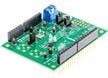
Analog Devices Inc. EVAL-AD5693RARDZ評価ボード
AD5693R回路のラピッドプロトタイピングが可能になり、設計時間を短縮できます。