


GOWIN LittleBee® GW1NR-9 FPGAs
GOWIN Semiconductor LittleBee® GW1NR-9 FPGAs allow for more efficiency with onboard memory and high-speed data rates. The GW1NR-9 FPGAs integrate an abundant pSRAM memory chip. The GW1NR series also implements low power consumption, instant-on, low cost, non-volatile, high security, various packages, and flexible usage. The GW1NR-9 FPGAs have been optimized with low power, small size, and the thinnest package as the design goal.
The GOWIN Semiconductor GW1NR-9 FPGAs are part of the LittleBee family of devices. LittleBee products are based on 55nm LP technology and offer instant-on, non-volatile, low-power, intensive I/O and a small footprint (2.4mm x 2.3mm). The LittleBee family is ideal for high-performance bridging applications and supports MIPI I3C and MIPI D-PHY as standard. This further reduces the board space and enhances performance.
The GW1NR-9 applies FPGA synthesizing, layout, place and routing, data bitstream generation, and downloads through GOWIN Semi's FPGA hardware development environment.
Features
- User Flash
- Up to 608 Kbits
- 10,000 write cycles
- Lower power consumption
- 55nm embedded flash technology
- LV: supports 1.2V core voltage
- UV: Built-in linear voltage regulator unit, unified power supply of VCC/ VCCX/ VCCO
- Clock dynamically turns on and off
- Integrate SDRAM/ PSRAM/ NOR FLASH
- Multiple I/O standards
- LVCMOS33/25/18/15/12; LVTTL33, SSTL33/25/18 I, SSTL33/25/18 II, SSTL15; HSTL18 I, HSTL18 II, HSTL15 I; PCI, LVDS25, RSDS, LVDS25E, BLVDSE
- MLVDSE, LVPECLE, RSDSE
- Input hysteresis option
- Supports 4mA, 8mA, 16mA, 24mA, etc. drive options
- Slew rate option
- Output drive strength option
- Individual bus keeper, weak pull-up, weak pull-down, and open drain option
- Hot socket
- BANK0 of GW1NR-9 supports MIPI Input
- BANK2 of GW1NR-9 supports MIPI Output
- BANK0 and BANK2 of GW1NR-9 support I3C OpenDrain/PushPull conversion
- High-performance DSP
- High-performance digital signal processing ability
- Supports 9 x 9, 18 x 18, 36 x 36 bits multiplier and 54 bits accumulator;
- Multipliers cascading
- Registers pipeline and bypass
- Adaptive filtering through signal feedback
- Supports barrel shifter
- Abundant slices
- Four-input LUT (LUT4)
- Double-edge flip-flops
- Supports shift register and distributed register
- Block SRAM with multiple modes
- Supports dual port, single port, and semi-dual port
- Supports bytes write enable
- Flexible PLLs
- Frequency adjustment (multiply and division) and phase adjustment
- Supports global clock
- Built-in flash programming
- Instant-on
- Supports security bit operation
- Supports AUTO BOOT and DUAL BOOT
- Configuration
- JTAG configuration
- Offers up to six GowinCONFIG configuration modes: AUTOBOOT, SSPI, MSPI, CPU, SERIAL, DUAL BOOT
Applications
- Embedded
- Server
Additional Resources
Specifications Chart

Associated Kit
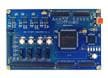
GOWIN DK-START-GW1NR9 V1.1 Development Kit
Designed to demonstrate the LittleBee® GW1NR-9 FPGAs with an integrated pSRAM memory chip.
Architecture Overview

Pinout

公開: 2020-07-20
| 更新済み: 2024-09-09