


Texas Instruments Texas Instruments LMK00301差動ファンアウトバッファ/レベルトランスレータ
Texas Instruments LMK00301差動ファンアウトバッファ/レベルトランスレータは、高周波数、低ジッタ、クロック/データ分配、レベル変換を意図しています。入力クロックは、2つのユニバーサル入力か1つのクリスタル入力を選択できます。選択された入力クロックは、5つの差動出力の2つのバンク、および1つのLVCMOS出力に分配されます。どちらの差動出力バンクも、LVPECL、LVDS、またはHCSLドライバ、あるいは無効化としてそれぞれに構成が可能です。LVCMOS出力では、イネーブル時またはディスエーブル時にラントパルス動作を防ぐために同期イネーブル入力を備えています。LMK00301は、1つの3.3Vコア電源と3つの独立した3.3V/2.5V出力電源で動作します。
特徴
- 3:1 Input multiplexer
- Two universal inputs operate up to 3.1GHz and accept LVPECL, LVDS, CML, SSTL, HSTL, HCSL, or single-ended clocks
- One crystal input accepts 10 to 40MHz crystal or a single-ended clock
- Two banks with 5 differential outputs each
- LVPECL, LVDS, HCSL, or Hi-Z (selectable per bank)
- LVPECL additive jitter with LMK03806 clock source at 156.25MHz: 20fs RMS (10kHz - 1MHz) 51fs RMS (12kHz - 20MHz)
- High PSRR of -65 / -76dBc (LVPECL/LVDS) at 156.25MHz
- LVCMOS Output with synchronous enable input
- Pin-controlled configuration
- 3.3V ± 5% VCC core supply
- 3 Independent VCCO output supplies at 3.3V/2.5V ± 5%
- -40°C to +85°C Industrial temperature range
- 48-lead WQFN (7mm × 7mm)
アプリケーション
- Clock distribution and level translation for ADCs, DACs, multi-Gigabit Ethernet, XAUI, fibre channel, SATA/SAS, SONET/SDH, CPRI, high-frequency backplanes, switches, routers, line cards, timing cards
- Servers, computing, PCI express (PCIe 3.0)
- Remote radio units and baseband units
Associated Eval Board
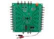
Texas Instruments LMK00301 Evaluation Board
Allows engineers to check the functional and performance verification of the LMK00301.
公開: 2015-12-15
| 更新済み: 2022-03-11